General technical page
C-Mode Scanning Acoustic Microscopy (C-SAM) Analysis
Discuss a C-SAM Investigation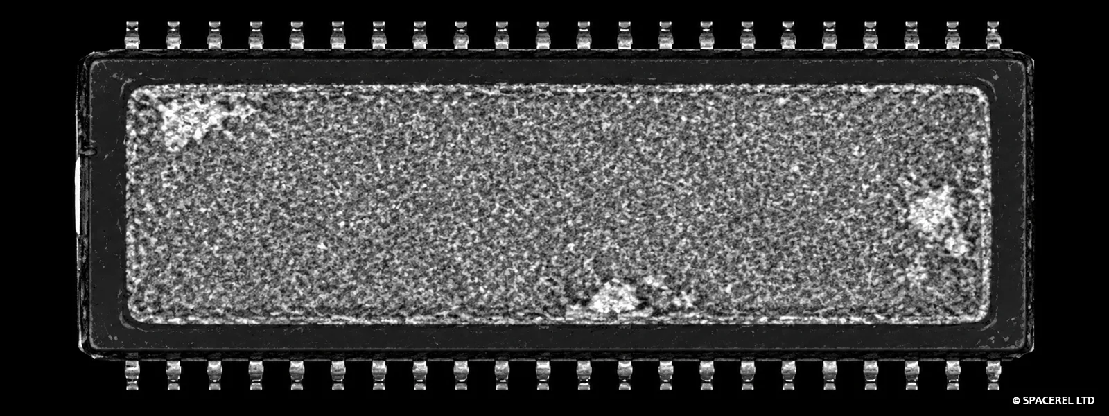
Non-Destructive Internal Inspection
Independent C-SAM Analysis with Engineering Interpretation
We provide an independent and technically rigorous C-Mode Scanning Acoustic Microscopy (C-SAM) service for non-destructive investigation of internal interfaces, bonding integrity and package-related defects in semiconductor devices and electronic components.
C-SAM uses high-frequency ultrasound to examine changes in acoustic response within a component. It is particularly sensitive to discontinuities at material interfaces, making it valuable for detecting delamination, voids, cracks, adhesion failures and other interface-related anomalies that may not be visible externally.
At SPACEREL, acoustic images are interpreted within the wider engineering context of the component. Package construction, manufacturing history, environmental exposure, reliability testing and other available evidence can all be considered when assessing whether an observed acoustic feature is relevant to the failure or reliability concern.
What Can C-SAM Reveal?
Acoustic waves are reflected, transmitted or scattered as they encounter changes in material properties and interfaces within a component. Interfaces containing an air gap can produce a particularly strong acoustic response, making acoustic microscopy highly effective for locating certain internal defects without physically opening or sectioning the package.
Typical applications include:
Delamination detection
Identify separation between mould compound, semiconductor die, die paddle, substrate, underfill or other bonded interfaces.
Void detection
Locate voids and air gaps within suitable adhesive, underfill, encapsulation and bonded structures.
Die-attach investigation
Assess bonding uniformity and identify areas of separation or voiding beneath a die where the package construction permits acoustic access.
Underfill inspection
Examine underfilled flip-chip and other packaged structures for voiding, delamination and bonding anomalies.
Crack detection
Detect some internal cracks where their orientation, size and acoustic contrast allow a measurable reflection.
Bondline assessment
Examine adhesive and bonded interfaces for discontinuities and areas of incomplete bonding.
Package integrity assessment
Compare internal acoustic features before and after manufacturing processes, environmental exposure or reliability testing.
Failed-versus-reference comparison
Compare equivalent regions of failed and known-good components to help determine whether an acoustic anomaly is associated with the failure.
C-SAM for Semiconductor Package Failure Investigation
Semiconductor packages contain multiple material interfaces that can be affected by assembly processes, moisture, thermal cycling, mechanical loading and differences in material expansion.
C-SAM provides a non-destructive way to examine these interfaces before destructive preparation is considered.
Typical investigations include:
- Die-to-mould-compound delamination
- Die-attach voiding or separation
- Die-paddle and leadframe interfaces
- Package cracking
- Mould-compound anomalies
- Underfill voiding and delamination
- Flip-chip package interfaces
- Bonding integrity
- Changes following reflow or environmental testing
- Comparison of failed and reference components
Identifying the location of an acoustic anomaly can also help define where subsequent cross-sectioning, FIB or other destructive analysis should be targeted.
C-SAM Detection of Package Delamination
C-SAM can reveal internal delamination within semiconductor packages by detecting changes in acoustic response at buried interfaces. In this scan, the brighter regions correspond to areas of delamination within the package, allowing their location and extent to be assessed non-destructively.
Die Attach, Underfill and Bonded Interface Inspection
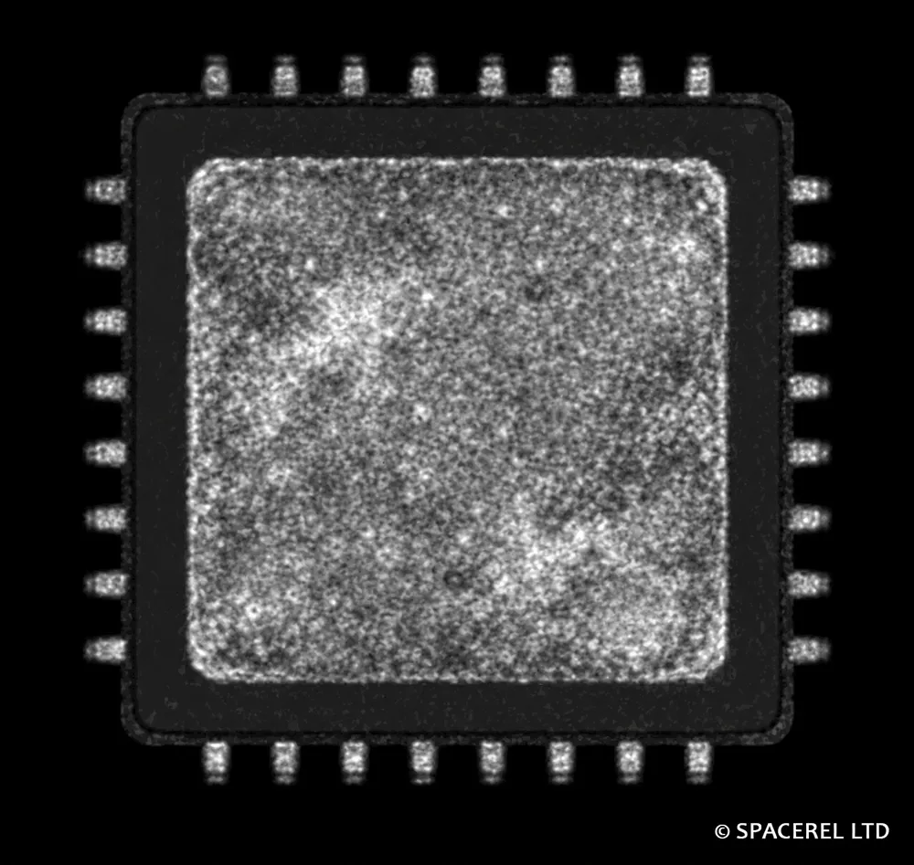
Bonded interfaces are one of the areas where C-SAM provides particularly useful information because even a very thin air gap can create a strong acoustic contrast.
Depending on the package construction and accessible acoustic path, C-SAM can support investigation of:
- Die-attach coverage and separation
- Underfill voids
- Underfill-to-die or underfill-to-substrate delamination
- Adhesive bondlines
- Mould-compound interfaces
- Bonded semiconductor structures
- Localised interface degradation
Acoustic findings should be interpreted against the known construction of the component. A strong reflection indicates an acoustic discontinuity, but additional evidence may be needed to determine why that discontinuity formed and whether it is responsible for the observed failure.
C-SAM for Wafer Bonding and Advanced Packaging
Acoustic microscopy can also support inspection of bonded wafers and advanced package structures where bond integrity and buried interfaces are important.
Practical applications can include:
- Bonded wafer interfaces
- Wafer-level packaging
- MEMS package structures
- 2.5D and 3D package interfaces
- Chiplet and heterogeneous integration
- Underfilled flip-chip structures
- Bond void investigation
As package complexity increases, C-SAM is often most useful as one part of a non-destructive inspection workflow rather than as a standalone technique.
Depth-Selective Acoustic Imaging
One of the useful features of C-mode acoustic microscopy is the ability to analyse acoustic information associated with a selected depth or interface within the component.
By controlling the acoustic focus and time gate, the investigation can concentrate on a particular internal plane rather than combining every reflection through the complete thickness of the sample.
This can help distinguish anomalies associated with different interfaces within a multilayer package and allows the scan strategy to be adapted to the package construction and the engineering question being investigated.
Pulse-Echo Measurement and Depth Selection
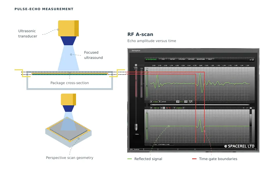
In pulse-echo acoustic microscopy, the transducer records reflected ultrasound as a function of time. The resulting A-scan contains responses from different depths and material interfaces within the component.
A time gate can be positioned around the response associated with a particular interface or depth range. As the transducer scans across the sample, the gated response is used to construct the C-mode image.
This allows the investigation to focus on a selected internal interface rather than combining acoustic information from the entire thickness of the package.
What Engineering Questions Can C-SAM Help Answer?
C-SAM is most useful when the inspection is driven by a specific question about package integrity or an internal interface.
Is there delamination inside the package?
Acoustic imaging can reveal regions where an interface has separated and produced a significant change in acoustic response.
Is the die attach continuous?
Depending on package construction, C-SAM can help identify voided or separated regions within the die-attach interface.
Is there evidence of underfill voiding?
Internal acoustic contrast can highlight voids and bonding anomalies within suitable underfilled structures.
Did reliability testing change the package?
Before-and-after scans can be compared following thermal cycling, reflow, humidity exposure or other stresses.
Is an anomaly localised or widespread?
C-mode imaging can show the lateral extent and distribution of an internal acoustic feature.
Where should destructive analysis be performed?
Acoustic inspection can identify a region of interest before cross-sectioning, FIB or other destructive preparation.
Is the same feature present in known-good components?
Comparison with reference samples can help determine whether an acoustic feature is unusual or associated with normal package construction.
Combining C-SAM with Other Failure Analysis Techniques
C-SAM is most powerful when its findings are correlated with other sources of evidence.
C-SAM can identify interface-related anomalies non-destructively. X-ray imaging can provide complementary information about dense internal structures and solder features. SEM, FIB and cross-sectioning can then provide higher-resolution physical examination where destructive analysis is justified.
This staged approach can help preserve evidence, reduce unnecessary destructive preparation and target subsequent analysis at the most relevant region of the component.
Scanning Electron Microscopy (SEM) Analysis
Our Approach to C-SAM Investigation
- 01
Define the Inspection Question
We establish the failure symptom, component construction, interfaces of interest and any relevant manufacturing, environmental or reliability-test history.
- 02
Review the Package Structure
The package configuration and expected internal interfaces are considered so that the acoustic inspection can be targeted appropriately.
- 03
Select the Scan Conditions
Suitable acoustic frequency, focus and depth range are selected according to the component geometry and the features being investigated.
- 04
Acquire the Acoustic Images
Relevant interfaces are scanned and significant acoustic features are documented.
- 05
Compare Regions and Samples
Where appropriate, suspect areas are compared with neighbouring regions, reference components or earlier scans.
- 06
Interpret the Evidence
Acoustic features are evaluated against package construction and the available engineering information to determine which observations are potentially significant.
- 07
Define Further Analysis
Where the acoustic findings require confirmation or deeper investigation, appropriate follow-on techniques can be recommended.
Non-Destructive Evidence for Engineering Decisions
The objective is not simply to provide an acoustic image. The inspection should help answer a defined engineering or reliability question.
Depending on the scope of the investigation, deliverables can include:
- C-SAM images of relevant internal interfaces
- Annotated areas of interest
- Identification of acoustic anomalies
- Failed-versus-reference comparisons
- Before-and-after reliability-test comparisons
- Assessment of delamination or void distribution where appropriate
- Interpretation of significant observations
- Discussion of relevant limitations or image artefacts
- Recommendations for targeted follow-on analysis
- Clear technical reporting
Findings can be presented in a technical report suitable for engineering review, supplier investigation, customer communication or wider root-cause analysis.
Where C-SAM Analysis Is Most Useful
C-SAM is particularly useful where reliability depends on the integrity of internal bonded interfaces or polymer-based package structures.
Common applications include:
Semiconductor Packaging
Plastic encapsulated devices, moulded packages, die attach, leadframe interfaces and package delamination.
Flip-Chip and Advanced Packaging
Underfill, bonded interfaces, stacked structures and heterogeneous package integration.
Power Electronics
Selected die-attach, bonded and encapsulated interfaces where acoustic access and material construction are suitable.
MEMS and Wafer-Bonded Devices
Bonded wafers, sealed structures and internal bond integrity.
Reliability and Qualification Testing
Comparison before and after thermal cycling, reflow, humidity exposure or other environmental stresses.
Manufacturing and Process Investigation
Assessment of bonding consistency, package defects and process-related interface anomalies.
C-SAM FAQ
Frequently Asked Questions
What Is C-SAM Analysis?
C-Mode Scanning Acoustic Microscopy uses high-frequency ultrasound to create depth-selective images of internal features and material interfaces. It is commonly used for non-destructive inspection of semiconductor packages and bonded structures.
Is C-SAM Non-Destructive?
Yes, the acoustic inspection itself is normally non-destructive. This makes C-SAM useful before destructive techniques such as cross-sectioning or FIB are considered.
What Defects Can C-SAM Detect?
C-SAM is particularly useful for detecting delamination, air gaps, voids, bonding anomalies and some cracks within suitable package and material structures.
Why Is C-SAM Sensitive to Delamination?
A delaminated interface often contains an air gap. The large difference in acoustic properties between air and the surrounding solid materials produces a strong reflection, making these interfaces readily detectable under suitable conditions.
Can C-SAM Inspect Die Attach?
Yes, where the package construction and acoustic path are suitable. C-SAM can help identify areas of incomplete bonding, separation or voiding within die-attach interfaces.
Can C-SAM Inspect Underfill?
Yes. Acoustic microscopy is used for examination of underfilled flip-chip structures and can reveal voiding or delamination at relevant interfaces.
Can C-SAM Determine the Root Cause of a Failure?
Not usually on its own. C-SAM can identify and localise internal acoustic anomalies, but determining why the anomaly formed and whether it caused the electrical failure normally requires other engineering evidence.
What Is the Difference Between C-SAM and X-Ray Inspection?
C-SAM is particularly sensitive to interface separation and air-gap defects within suitable structures. X-ray inspection is generally stronger for density-related features and metallic structures such as solder joints. The two techniques can therefore provide complementary information.
Can C-SAM Be Used Before and After Reliability Testing?
Yes. Comparing acoustic images before and after environmental or reliability testing can help identify changes such as new or increased delamination, provided the scans are performed under suitably comparable conditions.
Technical References
Further Reading
Connected expertise
Related capabilities and technical resources
Discuss the engineering challenge