General technical page
Focused Ion Beam (FIB) Analysis
Discuss a FIB Investigation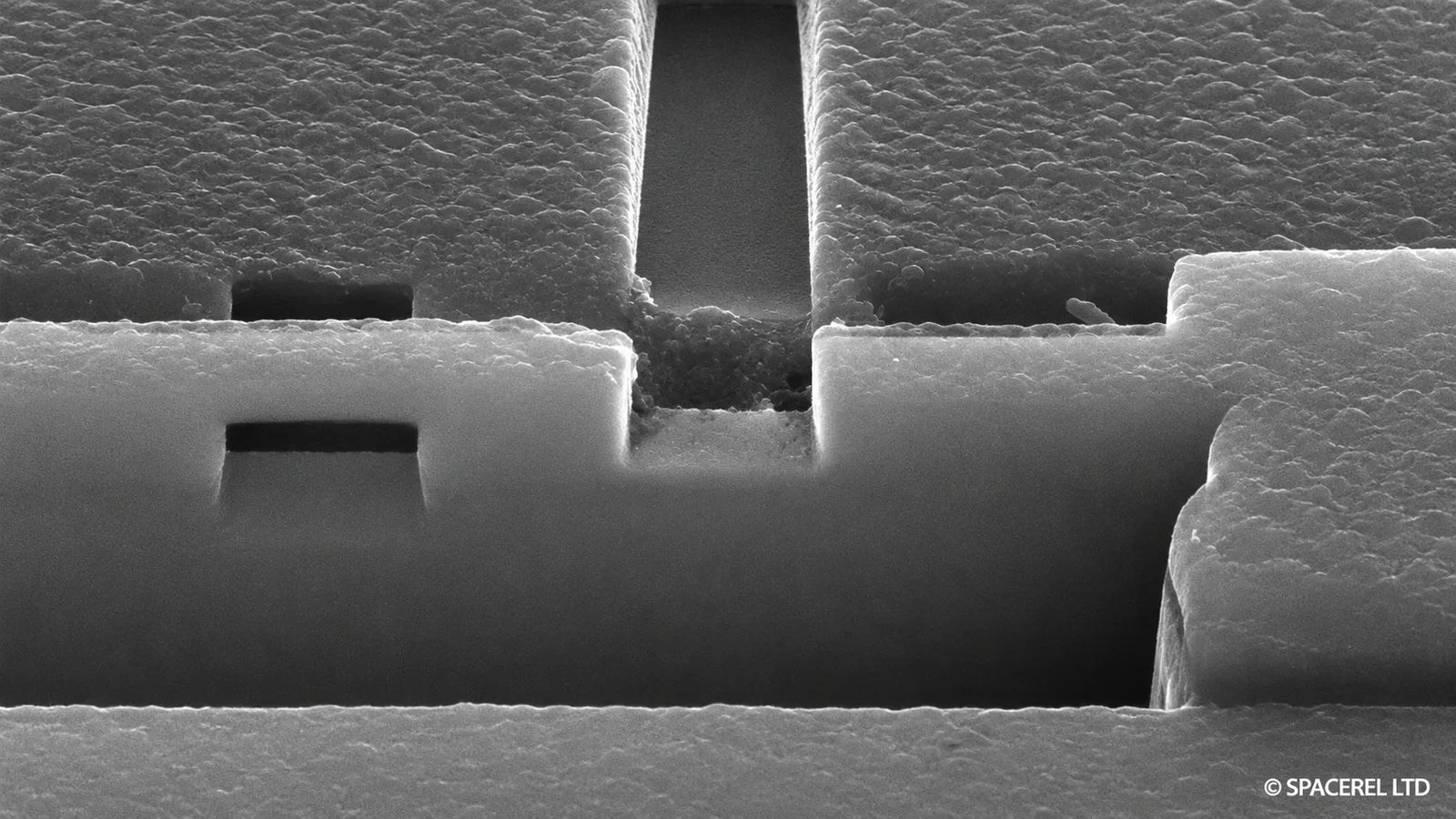
Site-Specific Analysis
Independent FIB Investigation with Engineering Interpretation
We provide an independent and technically rigorous failure investigation service using focused ion beam (FIB) techniques for precise, site-specific examination and preparation of microelectronic devices, electronic components and engineering materials.
FIB is particularly valuable when the feature of interest lies beneath the surface or when a specific microscopic region needs to be exposed, sectioned or prepared for further analysis. It can support investigations involving semiconductor structures, metallisation, interconnects, interfaces, cracks, voids, inclusions and manufacturing defects.
At SPACEREL, FIB is used as part of the wider failure investigation rather than simply as a material-removal process. FIB-prepared features can be examined alongside SEM, EDS, electrical test results, manufacturing information and other available evidence to help establish the most credible failure mechanism.
What Can Focused Ion Beam Analysis Reveal?
A focused ion beam uses a finely controlled beam of ions to remove material from a highly localised region. This allows buried structures and defects to be accessed with much greater positional control than conventional mechanical sectioning can provide.
FIB is particularly useful when the investigation needs to target a known microscopic feature without sectioning a much larger area of the sample.
Typical applications include:
Site-specific cross-sectioning
Expose a precise region of interest for examination of internal structures, interfaces or defects.
Semiconductor structure investigation
Examine metallisation, vias, contacts, dielectric layers, passivation and other microscopic device structures.
Defect exposure
Mill directly to a localised void, crack, particle, interface or suspected failure site identified during earlier examination.
TEM sample preparation
Prepare thin, site-specific lamellae from selected regions for subsequent transmission electron microscopy.
Layer and interface examination
Investigate multilayer structures, coatings, metallisation systems and buried interfaces.
Controlled material removal
Remove selected material to provide access to underlying features or structures.
3D investigation
Sequential milling and imaging can be used to build datasets for three-dimensional reconstruction of selected regions.
Preparation for complementary analysis
FIB-prepared sections can support further investigation using SEM, EDS, TEM or other analytical techniques.
Site-specific sample preparation and controlled milling are central FIB capabilities, including preparation of thin regions for TEM and other advanced microscopy
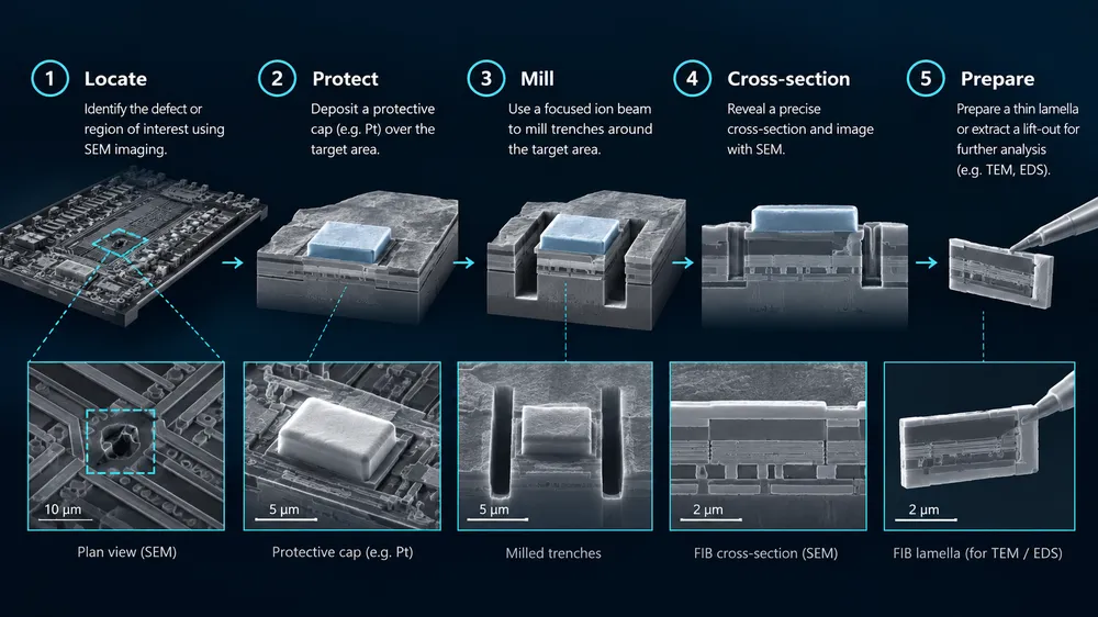
From Localised Defect to Site-Specific Analysis
A FIB investigation can progress from identifying the feature of interest to protective deposition, precision milling, cross-section exposure and preparation for further microscopic or compositional analysis.
The ability to target a specific microscopic region helps preserve the relationship between the suspected defect and the surrounding device or material structure while avoiding unnecessary preparation of unrelated areas.
FIB for Microelectronics and Semiconductor Failure Investigation
FIB is particularly valuable in semiconductor and microelectronic failure investigation because it allows precisely located features to be accessed without requiring a broad mechanical cross-section through the entire device.
A feature identified through electrical fault localisation, SEM imaging or another analytical technique can be targeted directly for physical examination.
Typical applications include:
- Metallisation defects
- Via and contact investigation
- Interconnect failures
- Dielectric and passivation structures
- Voids and buried defects
- Localised contamination
- Cracks and interface separation
- Semiconductor process anomalies
- Device structures beneath the surface
- Site-specific TEM lamella preparation
- Comparison of failed and reference structures
By exposing the selected internal structure, FIB can help connect an electrical or functional symptom with physical evidence located within the device.
FIB is widely used in semiconductor failure analysis and for preparation of specific device regions for higher-resolution examination.
Precision Cross-Sectioning of Localised Device Features
FIB allows a precisely selected region of a semiconductor or microelectronic structure to be milled and exposed for detailed examination. This is particularly useful where the feature of interest is buried beneath the surface or where conventional mechanical sectioning would not provide sufficient positional accuracy.
In this example, controlled ion-beam milling has created a localised cross-section at sub-micrometre scale, allowing the internal structure and interface geometry to be examined directly. This type of preparation can support investigation of metallisation, contacts, vias, dielectric structures, voids, cracks and other localised device features.
The exposed region can then be examined using SEM and, where appropriate, complementary techniques such as EDS or TEM to build a more complete understanding of the failure.
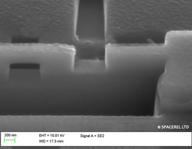
FIB for Electronic Components and Fine Interconnects
FIB can also support investigations of highly localised features within electronic components where precision cross-sectioning is required.
Applications can include:
- Fine metallic interconnects
- Component termination structures
- Thin metallic layers
- Localised interface defects
- Plated structures
- Micro-scale cracks
- Small voids or inclusions
- Embedded particles
- Thin coatings and layered structures
FIB becomes particularly valuable when the region of interest is too small or too position-sensitive for conventional sectioning techniques.
FIB for Materials Investigation
FIB can provide targeted access to microscopic features within engineering materials, allowing selected inclusions, interfaces, coatings, cracks or other localised features to be exposed for detailed examination.
Typical applications include:
- Coating and substrate interfaces
- Localised cracking
- Inclusions and second-phase features
- Thin films
- Porosity and voids
- Material interfaces
- Surface and subsurface defects
- Microstructural features
- Site-specific preparation for SEM, EDS or TEM
This targeted approach is particularly useful where a feature occupies only a small part of a larger sample and conventional preparation could miss, obscure or damage the area of interest.
FIB for Precision Component Investigation
FIB can support selected component and materials investigations where the critical evidence exists at very small scales.
Localised milling can expose subsurface cracks, coating interfaces, wear features, deposits or microstructural anomalies that are difficult to access through conventional preparation.
Potential applications include:
- Coating failures
- Micro-scale fracture features
- Wear surfaces
- Thin protective layers
- Corrosion interfaces
- Precision electrical contacts
- Localised inclusions
- Subsurface material defects
For larger-scale failures, conventional metallography or mechanical sectioning may be more appropriate. FIB is most valuable where precise access to a small and clearly defined region is required.
What Engineering Questions Can FIB Help Answer?
FIB analysis is most valuable when it is used to answer a clearly defined engineering question.
What lies beneath the visible surface defect?
FIB can remove material locally to expose the structure below a particle, crack, damaged region or other feature of interest.
Does a suspected defect continue below the surface?
A targeted cross-section can reveal the depth, geometry and relationship of a feature to the surrounding structure.
Is an interface intact?
Cross-sectioning can reveal local separation, voiding, cracking or structural changes across material interfaces.
Is a buried semiconductor feature associated with the failure?
FIB can target metallisation, contacts, vias or device regions identified during earlier localisation.
Can the region be prepared for higher-resolution analysis?
Site-specific material can be prepared for TEM or another advanced analytical technique.
Is the observed feature also present in a reference device?
Equivalent regions from failed and reference samples can be prepared and compared.
What analysis should follow?
The exposed structure can help determine whether SEM, EDS, TEM or another technique is needed to investigate the feature further.
Combining FIB with SEM and EDS
FIB, SEM and EDS provide complementary information during physical failure analysis.
FIB provides controlled access to the region of interest. SEM provides detailed imaging of the exposed structure. EDS can provide elemental information from selected features within the prepared region.
This combination can be particularly useful when investigating buried defects, metallisation systems, interfaces, particles and multi-material structures.
Rather than relying on a surface observation alone, the investigation can progress into the sample while maintaining precise control over where the cross-section is made.
Understanding What FIB Can and Cannot Tell You
FIB is a powerful preparation and investigation technique, but the process is inherently destructive because material is intentionally removed from the sample.
Important considerations include:
- The milled region is permanently altered
- Ion exposure can introduce localised preparation damage
- Material can redeposit during milling
- Very small or sensitive features may require protective deposition
- Milling conditions can influence the appearance of the prepared surface
- The exposed cross-section still requires engineering interpretation
- FIB alone does not normally establish the complete root cause of a failure
For these reasons, destructive FIB preparation should normally follow appropriate non-destructive examination and fault localisation where these steps are relevant.
Protective layers and suitable final preparation conditions can help reduce preparation artefacts in sensitive samples. JEOL, for example, describes protective deposition and lower-energy final milling as part of FIB TEM specimen preparation.
Our Approach to FIB Investigation
- 01
Define the Failure Question
We establish what needs to be exposed or prepared and review the available information from electrical testing, microscopy, manufacturing history or previous analysis.
- 02
Locate the Region of Interest
The target feature is identified as precisely as possible before destructive preparation begins.
- 03
Protect the Critical Feature
Where appropriate, a protective layer can be deposited over the region of interest to reduce preparation damage during subsequent milling.
- 04
Precision Milling
Material is removed in a controlled manner to expose the selected structure, interface or defect.
- 05
Examine the Cross-Section
The exposed region is documented and examined for relevant structures, defects and interfaces.
- 06
Perform Complementary Analysis
SEM, EDS, TEM or another analytical technique can be used where additional morphological, compositional or structural information is required.
- 07
Interpret the Evidence
Findings are considered alongside the original failure symptoms and other available engineering evidence to determine what conclusions are supported and what further investigation may be required.
Site-Specific Evidence for Engineering Decisions
The objective of FIB analysis is not simply to produce a cross-section. The prepared region should help answer a specific engineering question within the wider failure investigation.
Depending on the scope of the investigation, deliverables can include:
Images documenting the original region of interest
FIB cross-section images
Annotated structures and areas of concern
Failed-versus-reference comparisons
SEM examination of exposed features
Supporting EDS results where applicable
Documentation of observed defects and interfaces
Interpretation of relevant physical evidence
Discussion of preparation limitations or artefacts
Recommendations for further analysis
Clear technical reportingFindings can be presented in a technical report suitable for engineering review, supplier discussions, customer communication or wider root-cause investigation.
Where FIB Analysis Is Used
FIB is particularly valuable in industries where small, complex or highly integrated structures need to be examined at precise locations.
Semiconductor & Microelectronics
Integrated circuits, power devices, metallisation, contacts, vias, dielectric layers, hybrid circuits, multi-chip modules and semiconductor process investigation.
Electronics
Fine interconnects, component structures, coatings, interfaces and localised electronic defects.
Space & Aerospace
High-reliability electronic components where localised physical evidence can support failure and reliability investigations.
Defence
Electronic hardware and materials requiring detailed physical investigation of selected features.
Medical Devices
Microelectronic and precision components requiring controlled site-specific examination.
Energy & Harsh Environments
Components and materials where localised cracking, coating damage or interface degradation may contribute to failure.
Engineering Materials
Thin films, coatings, inclusions, microstructural features, cracks and material interfaces.
FIB FAQ
Frequently Asked Questions
Common questions about focused ion beam analysis, precision cross-sectioning, semiconductor failure investigation and site-specific sample preparation.
What Is Focused Ion Beam Analysis?
Focused ion beam analysis uses a finely focused beam of ions to remove or modify material from a precisely selected location. In failure analysis, it is commonly used for site-specific cross-sectioning, defect exposure and preparation of selected regions for further examination.
Is FIB Analysis Destructive?
Yes. FIB milling intentionally removes material, so the analysed region is permanently altered. The investigation sequence should therefore be planned carefully where sample preservation is important.
Why Is FIB Used in Semiconductor Failure Analysis?
Semiconductor devices contain very small and densely integrated structures. FIB allows a precisely selected region to be exposed without requiring a broad cross-section through the entire device, making it useful for investigating buried defects, metallisation, contacts, vias and other device features.
Can FIB Prepare Samples for TEM?
Yes. FIB is widely used for site-specific preparation of thin lamellae from selected regions for subsequent transmission electron microscopy.
Can FIB Be Used with SEM?
Yes. Dual-beam FIB-SEM systems combine ion-beam milling with electron-beam imaging, allowing material to be removed while the prepared region is monitored and examined.
Can EDS Be Performed on a FIB Cross-Section?
Yes, where the sample and analytical conditions are suitable. EDS can provide complementary elemental information from features exposed during FIB preparation.
Can FIB Determine the Root Cause of a Failure?
FIB can reveal important physical evidence by exposing buried structures and defects, but root-cause determination normally requires the findings to be considered alongside electrical behaviour, microscopy, material analysis, manufacturing information and other relevant evidence.
Can FIB Introduce Preparation Artefacts?
Yes. Ion-beam exposure and milling can alter the prepared region. Protective deposition, suitable milling conditions and lower-energy finishing can be used where appropriate to reduce preparation-related effects.
Technical References
Further Reading
Bassim, N., Scott, K. C. K. & Giannuzzi, L. A., Recent Advances in Focused Ion Beam Technology and Applications, MRS Bulletin, 2014.
Technical review covering FIB imaging, sectioning, specimen preparation, three-dimensional analysis and materials applications.
National Institute of Standards and Technology, Dual Beam Focused Ion Beam / Scanning Electron Microscope (FIB/SEM).
Overview of FIB-SEM capability including nanoscale milling, deposition, sample preparation and EDS analytical capability.
JEOL, Focused Ion-Beam Milling, FIB.
Technical overview of site-specific focused ion beam milling and TEM specimen preparation.
Connected expertise