General technical page
Scanning Electron Microscopy (SEM)
Discuss an SEM Investigation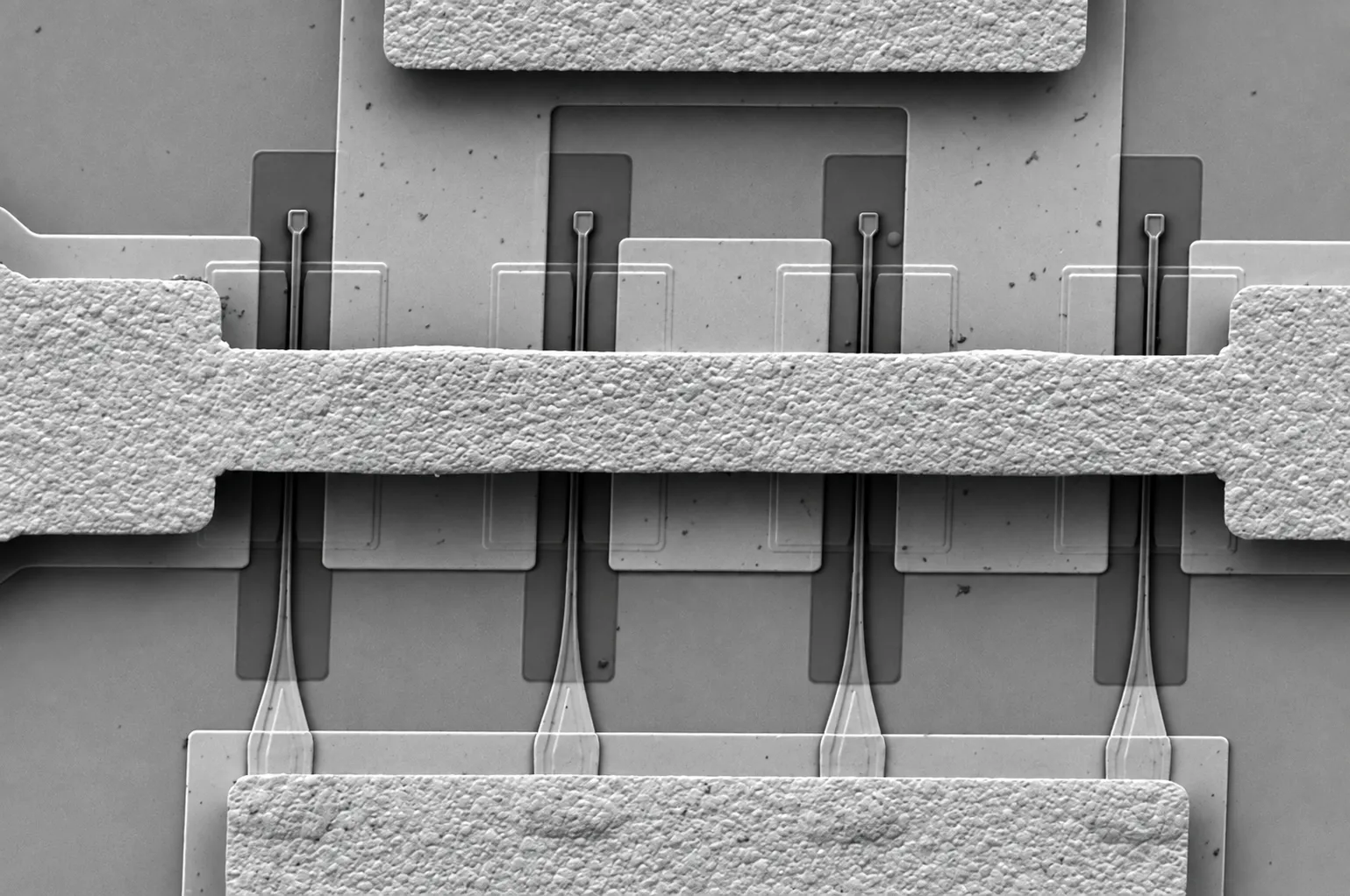
Independent SEM investigation with engineering interpretation
We provide an independent and technically rigorous failure investigation service using scanning electron microscopy (SEM) to examine defects, damage and material features that cannot be adequately resolved by conventional optical inspection.
Our focus is on producing clear, reliable and defensible evidence that can support root-cause investigations and engineering decisions. SEM can reveal fine surface features, fracture characteristics, contamination, material interfaces and manufacturing defects across microelectronics, semiconductor devices, electronic assemblies, engineering materials and mechanical components.
We look beyond the image itself. SEM observations are considered alongside the available design, manufacturing, test and service information to help establish the most credible failure mechanism and determine what further investigation may be required.
What can scanning electron microscopy reveal?
Scanning electron microscopy provides detailed imaging of surface morphology, fracture features and microstructural characteristics at much higher magnification and depth of field than conventional optical microscopy.
In failure analysis, this makes SEM particularly useful when the physical evidence associated with a defect or failure is too small, complex or subtle to characterise confidently by optical inspection alone.
Typical investigations include:
- Surface defects and morphology: cracks, pits, voids, deformation, wear, particles, deposits and localised surface damage.
- Fracture surfaces: examination of fracture origins and microscopic features associated with different failure mechanisms.
- Interfaces and cross-sections: investigation of material interfaces, coatings, solder joints, metallisation, die attach and layered structures following suitable sample preparation.
- Contamination and foreign material: localisation and examination of particles, deposits and residues.
- Corrosion and environmental damage: examination of corrosion morphology, surface attack and environmental degradation.
- Manufacturing defects: investigation of features associated with bonding, soldering, plating, coating, machining, assembly or material processing.
Where elemental composition is important, SEM imaging can be combined with energy-dispersive X-ray spectroscopy (EDS/EDX) to provide additional information about the elements present in a selected feature or region.
SEM for microelectronics and semiconductor failure investigation
SEM is particularly valuable in microelectronics when a failure involves physical features that cannot be resolved sufficiently using conventional microscopy.
Examination can be targeted at the semiconductor die, package, interconnects, bond interfaces and surrounding materials depending on the failure mode and the evidence available.
Typical applications include semiconductor die surface defects, metallisation and interconnect damage, passivation defects, wire bonds and bond pads, bond fracture surfaces, die-attach interfaces, particles and foreign material, package cracking, solder and interconnect failures, hybrid circuits, multi-chip modules and prepared device cross-sections.
SEM can also be used to compare failed and reference components, helping determine whether an observed feature is associated with the failure or represents normal construction, process variation or secondary damage.
Microfabricated Device and Interconnect Examination
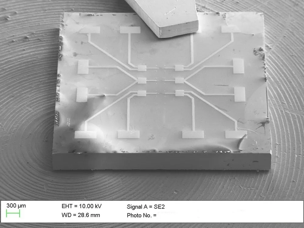
SEM can provide detailed examination of fabricated microelectronic structures, allowing patterned features, metallisation, contact regions and surface condition to be assessed at scales that are difficult to resolve using conventional optical microscopy.
This can support failure investigations involving fabrication defects, damaged or incomplete features, metallisation issues, contamination, surface damage and dimensional anomalies. SEM observations can also be correlated with electrical test results and process information to help determine whether a physical feature is relevant to the observed device behaviour.
SEM for electronic assemblies and components
At the component and assembly level, SEM can provide detailed physical evidence where electrical testing or optical inspection alone cannot explain a failure.
Investigations may involve solder joints, component terminations, PCB structures, connectors, contacts, plating systems, coatings, encapsulants and other electronic interfaces.
Potential applications include solder-joint fractures, intermetallic or interface features, PCB and via cross-sections, connector damage, plating defects, contamination, corrosion, cracked coatings and localised thermal or mechanical damage.
The greatest value normally comes from correlating the microscopic observations with the electrical symptoms, manufacturing history, environmental exposure and test conditions. This helps distinguish the observed damage from the underlying failure mechanism.
SEM for materials investigation
SEM can be used to examine the microstructure and failure surfaces of engineering materials where microscopic morphology provides information about how damage developed.
This can support investigations involving fracture, cracking, fatigue-related features, inclusions, porosity, coatings, corrosion, wear and material interfaces.
Particulate and Surface Contamination Analysis
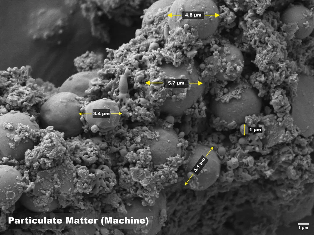
SEM provides high-resolution examination of particulate matter, surface deposits and other small material features that may be difficult to characterise using optical microscopy alone. Particle morphology, approximate dimensions, surface texture and the relationship between particles and the surrounding material can all provide useful evidence during a failure investigation.
This can support investigations involving contamination, process residues, wear debris, corrosion products, inclusions and unexpected foreign material. Where the composition of a particle or deposit is important, SEM examination can be combined with EDS elemental analysis to provide additional information about the elements present.
SEM for mechanical component failure investigation
Mechanical components can retain microscopic evidence of how a failure initiated and progressed even when the macroscopic fracture appears relatively simple.
SEM examination can support investigations involving unexpected fracture, fatigue, wear, corrosion, coating damage and manufacturing defects in components such as connectors, contacts, fasteners, springs, machined parts, metallic components and precision assemblies.
Material morphology and fracture examination
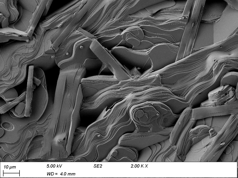
SEM can reveal fine surface and microstructural features that provide evidence about how a material has formed, degraded or failed. Features such as layered structures, fracture surfaces, cracking, deformation and local changes in morphology can be examined at micron-scale resolution.
This type of examination can support investigations involving fracture mechanisms, material degradation, coatings, composites, wear, process-related defects and unexpected structural features. The observations can then be correlated with material history, loading conditions and other analytical results to support the wider failure investigation.
What engineering questions can SEM help answer?
An SEM investigation should normally begin with an engineering question rather than simply a request for high-magnification images.
Where did the fracture originate?
Examination of the fracture surface may help identify initiation regions and features associated with how the damage propagated.
Is the defect associated with manufacturing or service exposure?
Surface morphology, fracture characteristics and comparison samples can provide evidence that helps distinguish between different possibilities.
Is contamination or foreign material present?
SEM can locate and characterise small particles or deposits, with EDS used where elemental information is required.
Is there evidence of corrosion, wear or environmental degradation?
SEM can reveal microscopic surface changes that are difficult to resolve optically.
Is the failure associated with an interface?
Prepared cross-sections can allow detailed investigation of solder joints, coatings, metallisation, die attach and other material interfaces.
What should be investigated next?
SEM findings can help determine whether further analysis such as EDS, cross-sectioning or another technique is justified.
SEM with EDS elemental analysis
High-resolution imaging can show where an unusual feature is located and what it looks like, but appearance alone cannot always establish what a material consists of.
Where elemental information is required, energy-dispersive X-ray spectroscopy (EDS or EDX) can be used alongside SEM to analyse the elements present in a selected area.
This can be useful when investigating contamination, corrosion products, inclusions, deposits, plating systems, foreign particles and unexpected material features.
Our approach to SEM failure investigation
Understand the failure
We first establish what failed, how the problem was detected and what evidence is already available. Electrical symptoms, operating conditions, manufacturing history, reliability testing and previous observations can all influence the investigation strategy.
Preserve the evidence
Failure evidence can be altered or destroyed by unnecessary handling or destructive preparation. The sequence of examination is therefore selected with the available samples and suspected failure mechanisms in mind.
Identify the area of interest
Optical inspection, electrical information or other non-destructive methods may be used to identify the regions most relevant to higher-resolution examination.
SEM examination
Relevant features are examined at appropriate magnifications and imaging conditions, with significant observations documented for subsequent interpretation.
Additional analysis where required
Depending on the findings, the investigation may progress to EDS, cross-sectioning or other analytical techniques rather than relying on SEM in isolation.
Engineering interpretation
Microscopy observations are evaluated alongside the available engineering evidence to determine what conclusions are supported, what alternative explanations remain possible and whether additional investigation is needed.
Clear evidence for engineering decisions
The objective is not simply to produce microscope images. The output should help you understand the problem and decide what to do next.
Depending on the scope of the investigation, deliverables can include high-resolution SEM images, annotated areas of interest, documented observations, failed-versus-reference comparisons, supporting EDS results where applicable, interpretation of the physical evidence, identification of potential failure mechanisms, limitations of the available evidence and recommendations for further investigation.
Findings can be provided in a clear technical report suitable for internal engineering review, supplier discussions, customer communication or wider root-cause investigations.
Where SEM failure investigation is used
Semiconductor & Microelectronics
ICs, semiconductor devices, packages, wire bonds, hybrid circuits, multi-chip modules and associated materials.
Electronics
PCBAs, solder joints, connectors, component terminations, coatings, encapsulants and electronic assemblies.
Space & Aerospace
High-reliability electronics and components where physical failure evidence needs to be understood and documented.
Defence
Electronic hardware, components and engineering materials requiring structured and independent failure investigation.
Medical Devices
Electronic and precision components where failure evidence needs to support engineering, quality or supplier investigations.
Energy & Harsh Environments
Components exposed to elevated temperature, vibration, corrosion, pressure or other demanding operating conditions.
Engineering Materials & Mechanical Components
Fractures, coatings, corrosion, wear, interfaces and manufacturing-related material defects.
SEM FAQ
Frequently asked questions
Common questions about SEM failure investigation, what the technique can reveal, sample preparation and when complementary analysis such as EDS may be required.
What is SEM failure analysis?
SEM failure analysis uses scanning electron microscopy to examine microscopic physical features associated with a failed component or material. It is particularly useful for investigating defects, fracture surfaces, contamination, corrosion, interfaces and microelectronic structures that cannot be adequately resolved using conventional optical microscopy.
Can SEM identify contamination?
SEM can locate and image small particles, deposits and residues. If elemental composition is required, SEM is commonly combined with EDS analysis to provide information about the elements present.
Can SEM be used for semiconductor failure analysis?
Yes. SEM can be used to examine semiconductor surfaces, metallisation, interconnects, bond pads, wire bonds, package structures, particles and other microscopic features associated with semiconductor and microelectronic failures.
Can SEM examine wire bonds and solder joints?
Yes. SEM can provide detailed examination of wire-bond, bond-pad and solder-joint surfaces, fractures and prepared cross-sections. The appropriate preparation method depends on the feature and failure mechanism being investigated.
Is SEM analysis destructive?
Not necessarily. Surface examination may require little alteration of the sample, although preparation requirements depend on the material and the feature being investigated. Analysis involving cross-sectioning, package opening or access to internal structures may be destructive.
Can SEM determine the root cause of a failure?
SEM can provide important physical evidence about a failure mechanism, but root-cause determination usually requires the microscopy findings to be considered alongside other information such as electrical behaviour, material analysis, manufacturing history, environmental exposure and reliability-test data.
When should EDS be used with SEM?
EDS is useful when the elemental composition of a particle, deposit, corrosion product or other feature is relevant to the investigation. SEM provides detailed imaging of the feature while EDS provides complementary elemental information.
Need to investigate a failure?
Have a failed component, unexplained defect or material issue? Discuss the problem with SPACEREL to determine whether SEM is the appropriate next step and what supporting analysis may be required.