General technical page
Energy-Dispersive X-ray Spectroscopy (EDS)
Discuss an EDS InvestigationElemental Analysis
Independent EDS Analysis with Engineering Interpretation
We provide an independent and technically rigorous elemental analysis service using energy-dispersive X-ray spectroscopy (EDS), also commonly referred to as EDX, to investigate the elemental composition of microscopic features, particles, deposits and material regions.
EDS is particularly valuable when visual examination alone cannot explain what a feature is made from or where an unexpected material may have originated. It can support investigations involving contamination, corrosion products, metallisation, plating, inclusions, process residues and material interfaces across semiconductors, microelectronics, electronic assemblies, engineering materials and mechanical components.
At SPACEREL, EDS results are considered alongside the available microscopy, design, manufacturing, test and service information. The objective is not simply to generate an elemental spectrum, but to understand what the result means within the wider failure investigation.
What Can Energy-Dispersive X-ray Spectroscopy Reveal?
EDS detects characteristic X-rays generated when a material is examined in an electron microscope. The resulting spectrum provides information about the elements present within the analysed region.
Depending on the investigation, EDS can be used for spot analysis, area analysis, line scans and elemental mapping, allowing the composition and distribution of selected elements to be compared across a feature or sample.
Typical applications include:
Elemental identification
Determine which detectable elements are present within a particle, deposit, surface feature or material region.
Contamination investigation
Compare unexpected particles or residues with surrounding materials and possible manufacturing or environmental sources.
Elemental mapping
Visualise the spatial distribution of selected elements across interfaces, structures, deposits or other areas of interest.
Material comparison
Compare failed and reference samples, different regions of the same component, or suspect material against known construction.
Corrosion products
Examine the elemental constituents associated with corrosion, deposits and environmentally induced surface changes.
Metallisation and plating
Investigate metallic layers, contact systems, coatings and unexpected elemental signatures.
Cross-section analysis
Combine EDS with prepared cross-sections to examine elemental distribution through layered structures and interfaces.
EDS Spectrum and Elemental Identification
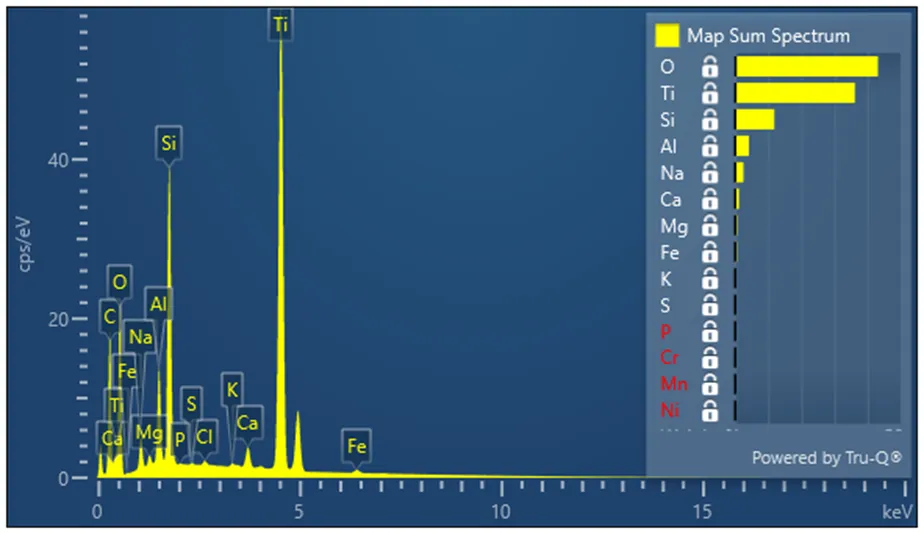
An EDS spectrum shows the characteristic X-ray peaks generated by the elements present within the analysed region. The position and intensity of these peaks provide information about which elements have been detected and their relative contribution to the measured signal.
In this example, the spectrum shows strong signals from oxygen and titanium, together with silicon, aluminium and several additional elements at lower levels. Interpreting these peaks alongside the SEM image and elemental maps helps build a clearer picture of the material composition and the distribution of features within the area under investigation.
EDS for Microelectronics and Semiconductor Failure Investigation
In semiconductor and microelectronic failure analysis, EDS can provide compositional information from highly localised features that may be difficult to understand from imaging alone.
This is particularly useful when SEM examination reveals an unexpected particle, residue, damaged region or area of unusual contrast, but its physical appearance does not explain its composition or possible origin.
Typical applications include:
- Foreign particles on semiconductor surfaces
- Bond-pad contamination
- Metallisation and contact materials
- Wire-bond interfaces
- Package residues and deposits
- Corrosion products
- Plating and surface finishes
- Die-attach and packaging materials
- Process-related contamination
- Cross-sectional material interfaces
- Comparison of failed and reference devices
EDS can help establish whether an unexpected feature is compositionally different from the surrounding structure and whether its elemental signature is consistent with a process material, environmental contaminant, corrosion product or another potential source.
EDS for Electronic Components and Assemblies
Electronic failures can involve particles, residues, corrosion products or material interfaces that cannot be fully understood through optical or electron microscopy alone.
EDS can provide localised elemental information from PCBAs, solder joints, connectors, contacts, component terminations, coatings, plated surfaces and other electronic structures.
Applications can include:
- Solder-joint and termination analysis
- Connector and contact investigation
- Plating and surface-finish assessment
- Corrosion deposits
- PCB contamination
- Process residues
- Metallic debris
- Component surface deposits
- Conductive particles
- Coating and interface investigation
When combined with SEM imaging, EDS allows the physical location and morphology of a feature to be correlated with its elemental composition, providing a stronger basis for engineering interpretation.
EDS for Materials Investigation
EDS can support materials investigations where the elemental composition of a local feature is important to understanding a defect, material anomaly or potential failure mechanism.
Analysis can be targeted to particles, inclusions, phases, corrosion products, coatings, deposits and interfaces identified during microscopic examination.
Typical applications include:
- Foreign material investigation
- Particulate contamination
- Inclusions and unexpected phases
- Corrosion products
- Wear debris
- Coating composition
- Surface deposits
- Material interfaces
- Comparison of suspect and reference material
Combining morphological information from SEM with elemental information from EDS can help determine whether an observed feature is relevant to the failure or simply part of the normal material structure.
Correlating Material Features with Elemental Composition
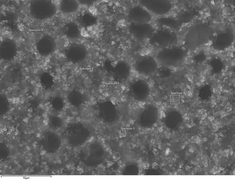
EDS is most useful when elemental information is considered alongside the physical features visible in the SEM image. Surface morphology, particles, deposits and compositionally distinct regions can first be identified visually, then targeted for elemental analysis.
In this example, the SEM image provides the structural context for the same region examined by EDS. Comparing the morphology with the elemental maps and spectrum helps determine whether particular features are associated with changes in composition and whether they warrant further investigation.
EDS for Mechanical Component Failure Investigation
Mechanical failures can retain localised material and environmental evidence that benefits from elemental analysis.
EDS can support investigations involving corrosion products, transferred material, wear debris, coatings, surface deposits and unexpected particles found on damaged or fractured mechanical components.
Applications may include connectors, contacts, fasteners, springs, machined components, metallic assemblies, coated surfaces and precision mechanical parts.
EDS results can be considered alongside fracture morphology, operating environment, material specification and service history to help build a more complete picture of the failure.
What Engineering Questions Can EDS Help Answer?
EDS analysis is most valuable when it is used to answer a specific engineering question rather than simply generate a spectrum.
What is this particle or deposit made from?
EDS can identify the detectable elements present and help compare the feature with surrounding or known materials.
Is the contamination consistent with a process material?
Elemental composition can help assess whether a particle or residue is consistent with solder, plating, metallic debris, environmental contamination or another possible source.
Does the failed area differ from a reference sample?
Comparative EDS analysis can reveal elemental differences between failed, unaffected and reference regions.
What elements are associated with a corrosion product?
Localised analysis can identify the elemental constituents associated with corrosion or surface deposits.
Is the coating or plating consistent across the sample?
Spot analysis, line scans or elemental mapping can be used to compare different locations or interfaces.
Where is a particular element located?
Elemental mapping can show the spatial distribution of selected elements across the analysed region.
Is further analysis required?
EDS can narrow the investigation, but additional analytical techniques may be needed where molecular structure, oxidation state, trace-level chemistry or precise material identification is important.
Combining SEM Imaging with EDS Elemental Analysis
SEM and EDS are commonly used together because they provide complementary information.
SEM shows the morphology, location and physical structure of a feature. EDS provides information about the elements present within that feature.
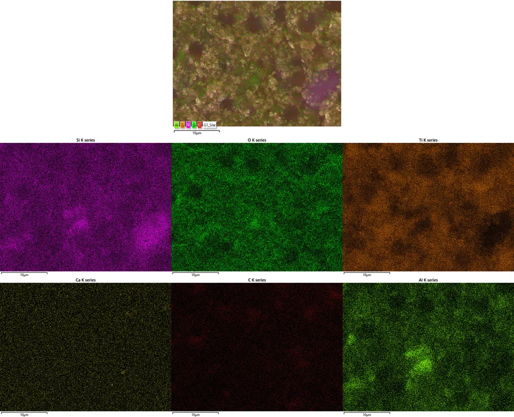
Elemental mapping can then show how selected elements are distributed across the same analysed region. By comparing the composite image with individual elemental maps, compositionally distinct areas, localised features and material variations can be identified more clearly.
In this example, the maps show the distribution of oxygen, aluminium, silicon, titanium and iron across the analysed area. Interpreting these distributions alongside the SEM image and EDS spectrum provides a stronger basis for understanding the material and deciding whether further investigation is required.
Combining SEM Imaging with EDS Elemental Analysis
SEM and EDS are commonly used together because they provide complementary information.
SEM shows the morphology, location and physical structure of a feature. EDS provides information about the elements present within that feature.
For example, SEM may reveal an unexpected particle on a bond pad, semiconductor surface or connector. EDS can then be targeted to the particle and surrounding regions to determine whether their elemental signatures differ and whether the result supports a particular contamination or material-origin hypothesis.
Combining morphology with elemental composition can provide a much stronger basis for failure investigation than interpreting either source of evidence in isolation.
Understanding What EDS Can, and Cannot, Tell You
EDS is a powerful elemental analysis technique, but its results need to be interpreted within the limitations of the method and the sample being examined.
EDS primarily provides information about which elements are present. It does not normally identify the exact chemical compound, molecular structure or oxidation state of a material on its own.
The analysed volume can also extend beneath or around the visible feature, meaning that signals from the underlying or adjacent material may contribute to the spectrum. Feature size, sample geometry, accelerating voltage, surface coatings and overlapping X-ray peaks can all influence the result.
Quantitative or semi-quantitative results should therefore be considered in context, particularly when analysing very small particles, thin films, layered structures or complex material systems.
Recognising these limitations is an important part of producing technically defensible conclusions from EDS data.
Our Approach to EDS Investigation
Step 1: Define the Analytical Question
We establish what needs to be understood, such as the composition of an unexpected particle, whether two regions differ, or whether a deposit is consistent with a suspected material source.
Step 2: Locate the Feature
SEM or optical examination is used to identify and document the relevant area before elemental analysis is performed.
Step 3: Select the Appropriate EDS Method
Depending on the investigation, analysis may involve individual points, selected areas, line scans or elemental mapping.
Step 4: Compare Relevant Regions
Where possible, suspect features are compared with surrounding material, known construction or reference samples rather than interpreted in isolation.
Step 5: Interpret the Results
Spectra and elemental maps are reviewed alongside the physical morphology, sample construction and known materials to determine what conclusions are supported by the evidence.
Step 6: Define the Next Step
Where EDS cannot resolve the engineering question on its own, further analysis or sample preparation can be recommended.
Clear Elemental Evidence for Engineering Decisions
The objective is not simply to provide spectra or colourful elemental maps. The results should help answer the engineering question behind the investigation.
Depending on the scope of the work, deliverables can include:
- SEM images documenting the analysed regions
- EDS spectra from selected points or areas
- Identification of detected elements
- Elemental maps
- Line-scan results where appropriate
- Failed-versus-reference comparisons
- Annotated areas of interest
- Interpretation of significant elemental findings
- Discussion of limitations and alternative explanations
- Recommendations for additional investigation where appropriate
- Clear technical reporting
Findings can be presented in a technical report suitable for engineering review, supplier discussions, customer communication or wider root-cause investigation.
Where EDS Elemental Analysis Is Used
EDS is used across a wide range of industries where understanding the elemental composition of microscopic features can support failure investigation, quality assessment and engineering decision-making.
Semiconductor & Microelectronics
Semiconductor devices, metallisation, bond pads, packages, wire bonds, hybrid circuits, multi-chip modules and process-related contamination.
Electronics
PCBAs, solder joints, connectors, component terminations, coatings, plating and electronic assemblies.
Space & Aerospace
High-reliability electronic hardware where contamination, corrosion or material composition may affect performance or reliability.
Defence
Electronic components, assemblies and engineering materials requiring structured failure investigation.
Medical Technology
Electronic and precision components where material or contamination evidence supports engineering, quality or supplier investigations.
Energy & Harsh Environments
Components exposed to elevated temperature, corrosion, pressure, contamination or other demanding environmental conditions.
Engineering Materials & Mechanical Components
Corrosion products, coatings, inclusions, wear debris, deposits and material interfaces.
EDS FAQ
Frequently Asked Questions
Common questions about EDS elemental analysis, contamination investigation, elemental mapping and how EDS is used alongside SEM.
What Is EDS Analysis?
Energy-dispersive X-ray spectroscopy (EDS) is an analytical technique commonly used with scanning electron microscopy to identify the elements present within a selected region of a sample.
Is EDS the Same as EDX?
Yes. EDS and EDX are commonly used names for the same general technique: energy-dispersive X-ray spectroscopy.
Can EDS Identify Contamination?
EDS can identify the detectable elements present in a particle, residue or deposit. This can help determine whether its composition is consistent with a suspected contamination source, although additional analysis may sometimes be required for definitive material identification.
Can EDS Identify an Exact Chemical Compound?
Not usually on its own. EDS primarily provides elemental information rather than molecular structure, chemical bonding or oxidation state. Other analytical techniques may be required where exact compound identification is necessary.
Can EDS Analyse Very Small Particles?
Yes, EDS can be targeted to microscopic features, but the effective analysis volume may extend beyond the visible particle. Particle size, underlying material, sample geometry and operating conditions therefore need to be considered when interpreting the result.
What Is an EDS Elemental Map?
An elemental map shows the spatial distribution of selected elements across an analysed area. This can be particularly useful for examining interfaces, contamination, deposits and multi-material structures.
Why Is EDS Commonly Used with SEM?
SEM provides detailed information about the location, shape and morphology of a feature, while EDS provides complementary elemental information. Using the techniques together can provide a more complete understanding of a defect or failure.
Is EDS Quantitative?
EDS can provide quantitative or semi-quantitative composition estimates under suitable conditions, but accuracy depends on factors including sample geometry, feature size, surface condition, operating conditions and spectral interpretation.
Connected expertise